Interfacing ADC to 8051
ADC (Analog to digital converter) forms a very essential part in many embedded projects and this article is about interfacing an ADC to 8051 embedded controller. ADC 0804 is the ADC used here and before going through the interfacing procedure, we must neatly understand how the ADC 0804 works.
ADC 0804.
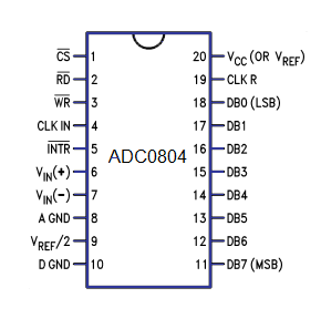
ADC0804 is an 8 bit successive approximation analogue to digital converter from National semiconductors. The features of ADC0804 are differential analogue voltage inputs, 0-5V input voltage range, no zero adjustment, built in clock generator, reference voltage can be externally adjusted to convert smaller analogue voltage span to 8 bit resolution etc. The pin out diagram of ADC0804 is shown in the figure below.
The voltage at Vref/2 (pin9) of ADC0804 can be externally adjusted to convert smaller input voltage spans to full 8 bit resolution. Vref/2 (pin9) left open means input voltage span is 0-5V and step size is 5/255=19.6V. Have a look at the table below for different Vref/2 voltages and corresponding analogue input voltage spans.
Vref/2 (pin9) (volts) | Input voltage span (volts) | Step size (mV) |
Left open | 0 – 5 | 5/255 = 19.6 |
2 | 0 – 4 | 4/255 = 15.69 |
1.5 | 0 – 3 | 3/255 = 11.76 |
1.28 | 0 – 2.56 | 2.56/255 = 10.04 |
1.0 | 0 – 2 | 2/255 = 7.84 |
0.5 | 0 – 1 | 1/255 = 3.92 |
Steps for converting the analogue input and reading the output from ADC0804.
- Make CS=0 and send a low to high pulse to WR pin to start the conversion.
- Now keep checking the INTR pin. INTR will be 1 if conversion is not finished and INTR will be 0 if conversion is finished.
- If conversion is not finished (INTR=1) , poll until it is finished.
- If conversion is finished (INTR=0), go to the next step.
- Make CS=0 and send a high to low pulse to RD pin to read the data from the ADC.
Circuit diagram.
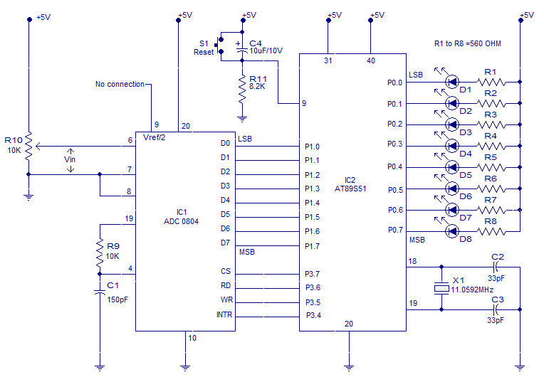
The figure above shows the schematic for interfacing ADC0804 to 8051. The circuit initiates the ADC to convert a given analogue input , then accepts the corresponding digital data and displays it on the LED array connected at P0. For example, if the analogue input voltage Vin is 5V then all LEDs will glow indicating 11111111 in binary which is the equivalent of 255 in decimal. AT89s51 is the microcontroller used here. Data out pins (D0 to D7) of the ADC0804 are connected to the port pins P1.0 to P1.7 respectively. LEDs D1 to D8 are connected to the port pins P0.0 to P0.7 respectively. Resistors R1 to R8 are current limiting resistors. In simple words P1 of the microcontroller is the input port and P0 is the output port. Control signals for the ADC (INTR, WR, RD and CS) are available at port pins P3.4 to P3.7 respectively. Resistor R9 and capacitor C1 are associated with the internal clock circuitry of the ADC. Preset resistor R10 forms a voltage divider which can be used to apply a particular input analogue voltage to the ADC. Push button S1, resistor R11 and capacitor C4 forms a debouncing reset mechanism. Crystal X1 and capacitors C2,C3 are associated with the clock circuitry of the microcontroller.
Program.
ORG 00H
MOV P1,#11111111B // initiates P1 as the input port
MAIN: CLR P3.7 // makes CS=0
      SETB P3.6 // makes RD high
      CLR P3.5 // makes WR low
      SETB P3.5 // low to high pulse to WR for starting conversion
WAIT: JB P3.4,WAIT // polls until INTR=0
      CLR P3.7 // ensures CS=0
      CLR P3.6 // high to low pulse to RD for reading the data from ADC
      MOV A,P1 // moves the digital data to accumulator
      CPL A // complements the digital data (*see the notes)
      MOV P0,A // outputs the data to P0 for the LEDs
      SJMP MAIN // jumps back to the MAIN program
      END
Notes.
- The entire circuit can be powered from 5V DC.
- ADC 0804 has active low outputs and the instruction CPL A complements it t0 have a straight forward display. For example, if input is 5V then the output will be 11111111 and if CPL A was not used it would have been 00000000 which is rather awkward to see.


No comments:
Post a Comment