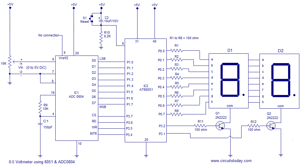
Voltmeter using 8051.
A simple 0-5V voltmeter using 8051 is shown in this article. This digital voltmeter has a sensitivity of 200mV which is a bit low but this project is meant for demonstrating how an ADC and seven segment display can be interfaced to 8051 to obtain a digital readout of the input voltage. A 31/2 digit high end voltmeter will be added soon. ADC0804 is the ADC and AT89S51 is the controller used in this project. Before attempting this project, go through these projects Interfacing ADC to 8051 and Interfacing seven segment display to 8051 which will give you a good idea on the basics.
Circuit diagram.

About the circuit.
In the circuit Vref/2 (pin9) of the ADC is left open and it means that the input voltage span can be o to 5V and the step size will be 5/255 = 19.6mV. The equation for the digital output of ADC0804 is Dout = Vin/Step size. In this circuit, for an input voltage of 1V the digital output will be 1/19.6mV = 51 and so the binary equivalent of 51 ie 00110011. Digital output of the ADC is interfaced to P1.0 of the microcontroller. Control signals for the ADC ie CS, RD, WR and INTR are available from the P3.7, P3.6, P3.5 and P3.4 pins of the microcontroller respectively. 2 digit multiplexed seven segment display is interfaced to Port0 of the microcontroller. Control signals for the display driver transistors Q1 and Q2 are obtained from P3.2 and P3.1 of the microcontroller. Push button switch S1, capacitor C2 and resistor R10 forms a debouncing reset circuitry.
Program.
ORG 00H
MOV P1,#11111111B
MOV P0,#00000000B
MOV P3,#00000000B
MOV DPTR,#LABEL
MAIN: CLR P3.7
SETB P3.6
CLR P3.5
SETB P3.5
WAIT: JB P3.4,WAIT
CLR P3.7
CLR P3.6
MOV A,P1
MOV B,#10D
DIV AB
MOV B,#2D
MUL AB
MOV B,#10D
DIV AB
SETB P3.2
ACALL DISPLAY
MOV P0,A
ACALL DELAY
MOV P0,#10000000B
ACALL DELAY
MOV A,B
CLR P3.2
SETB P3.1
ACALL DISPLAY
MOV P0,A
ACALL DELAY
CLR P3.1
SJMP MAIN
DELAY: MOV R3,#02H
DEL1: MOV R2,#0FAH
DEL2: DJNZ R2,DEL2
DJNZ R3,DEL1
RET
DISPLAY: MOVC A,@A+DPTR
RET
LABEL: DB 3FH
DB 06H
DB 5BH
DB 4FH
DB 66H
DB 6DH
DB 7DH
DB 07H
DB 7FH
DB 6FH
END
About the program.
At first the program controls the ADC to produce a digital output corresponding to the input voltage.This digital output is scanned through P1.0 and is loaded to accumulator. Then the value in the accumulator is divided by 10 to omit the last digit. For example, let the input voltage be 4V. Then the corresponding digital output of the ADC will be 204D (D stands for decimal) .After the the division by 10, the value left in the accumulator will be 20D. This 20D is then multiplied by 2D which results in 40D. The next target of the program is to manipulate this 40D and make a 4.0 readout on the display. For this the 40D is again divided by 10D . This results in 4 inside accumulator and 0 inside B register. Then the program gets the digit drive pattern for 4 using the lookup table , puts this pattern on Port 0 and activates Q1. After 1 ms delay 10000000B is loaded to P0 and this accounts for the dot. After a further 1ms delay Q1 is deactivated, content in B (ie 0) is moved to A, gets the correct digit drive pattern for 0 using the lookup table, puts this pattern on Port 0 and activates Q2. After a further 1ms delay Q2 is deactivated and the entire cycle is repeated.


No comments:
Post a Comment