This article is about a simple heart rate monitor using 8051 microcontroller. Like the previous 8051 projects, AT89S51 is the microcontroller used here. The device senses the heart rate from the finger tip using IR reflection method and displays it on a three digit seven segment display in beats per minute. The circuit has an accuracy of 4 beats per minute and it is very easy to use. In medical terms, the technique used here for sensing heart rate is called photoplethysmography.
Photoplethysmography.
Photoplethysmography is the process of optically estimating the volumetric measurement of an organ. Pulse oximetry, cardiovascular monitoring, respiration detection, heart rate monitoring etc are few common applications of photoplethysmography. Let us have a look at the application of photoplethysmography in heart rate monitoring from the figer tip. When the heart expands (diastole) the volume of blood inside the finger tip increases and when the heart contrcats (systole) the volume of blood inside the finger tip decreases. The resultant pulsing of blood volume inside the finger tip is directly proportional to the heart rate and if you could some how count the number of pulses in one minute, that’s the heart rate in beats per minute (bpm). For this an IR transmitter/receiver pair placed in close contact with the finger tip. When the heart beats, the volume of blood cells under the sensor increases and this reflects more IR waves to sensor and when there is no beat the intensity of the reflected beam decreases. The pulsating reflection is converted to a suitable current or voltage pulse by the sensor. The sensor output is processed by suitable electronic circuits to obtain a visible indication (digital display or graph).
Heart rate monitor using 8051.
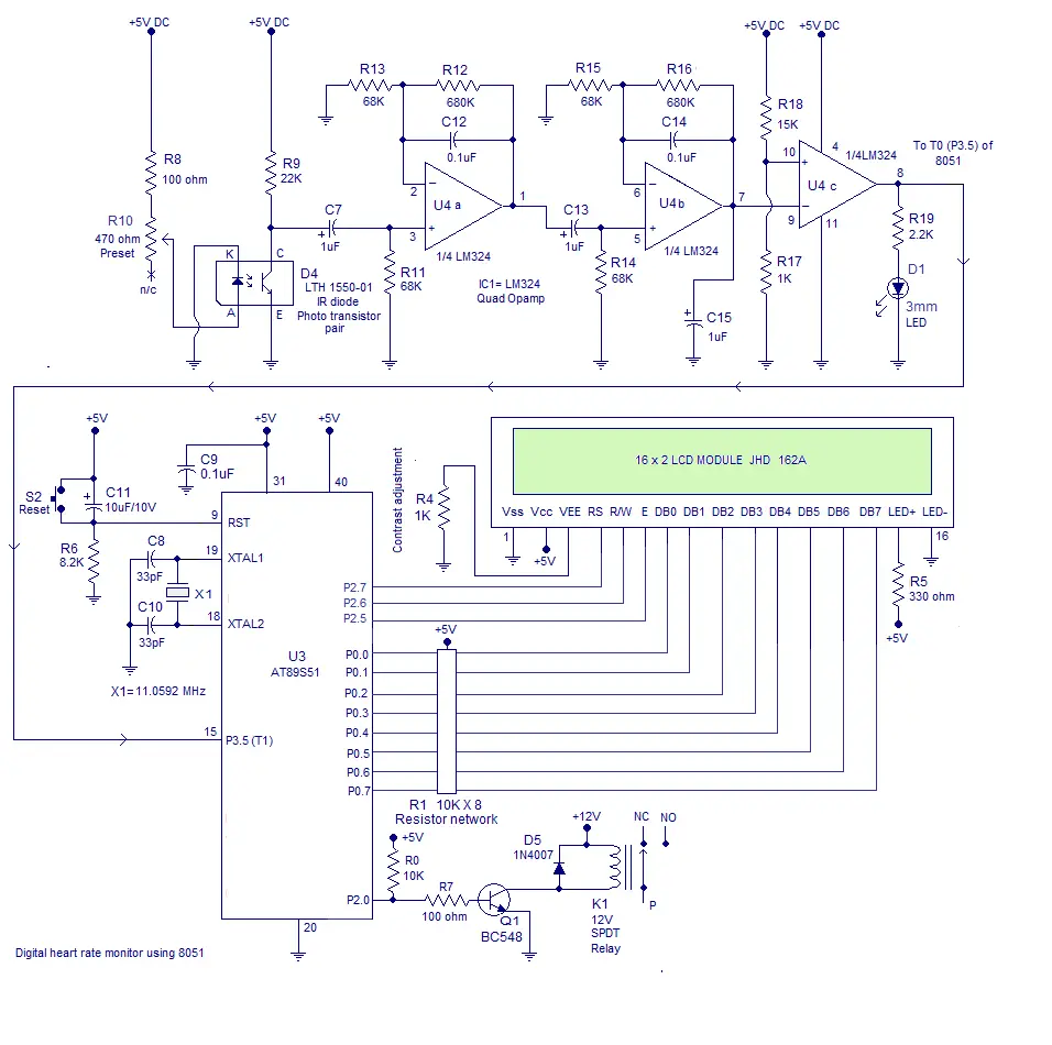
Circuit diagram.
Working of the heart rate monitor
LTH1550-01 photo interrupter forms the photoplethysmographic sensor here. LTH1550-01 is simply a IR diode – photo transistor pair in single package. The front side of the IR diode and photo transistor are exposed and the remaining parts are well isolated. When the finger tip is placed over the sensor the volumetric pulsing of the blood volume inside the finger tip due to heart beat varies the intensity of the reflected beam and this variation in intensity is according to the heart beat.
When more light falls on the photo transistor it conducts more, its collector current increases and so its collector voltage decreases. When less light falls on the photo transistor it conducts less, its collector current decreases and so its collector voltage decreases. This variation in the collector voltage will be proportional to the heart rate. Any way this voltage variation is so feeble and additional signal conditioning stages are necessary to convert it into a microcontroller recognizable form.
The next part of the circuit consists of a two active low pass filters using opamp LM324. The LM324 is a quad opamp that can be operated from a single rail supply. Resistor R23, R17 and capacitor C5 sets the gain and cut off frequency of the first filter. With the given component values, gain will be 11 and cut off frequency will be 2.5Hz. The gain and cut off frequency are determined using the following equations. Capacitor C15 is used to by-pass noise if any may cause false triggering of the comparator.
Voltage gain Av =1 + (R17 / R23)
Cut off frequency Fc= 1/(2π *R17*C5)
The second low pass filter also have same gain and cut off frequency. The two low pass filters form a very critical part of the circuit as any noise or false signals passing to the microcontroller stage will produce disastrous results. The output of the filter stage will be a voltage level fluctuating between 0 and 0.35 volts and this fluctuation is converted into a 0 to 5V swing using the comparator based on the third opamp (IC1c). The reference voltage of the comparator is set to 0.3V. When ever the output voltage of the filter stage goes above 0.3V, the output of the comparator goes to zero and whenever the output voltage of the filter stage goes below 0.3V, the output of the comparator goes to positive saturation. The result will be a neat pulse fluctuating between 0 and 5V at a rate equal to the heart rate. This pulse is fed to the microcontroller for counting.
Program.
ORG 000H                   // origin
MOV DPTR,#LUT              // moves starting address of LUT to DPTR
MOV P1,#00000000B          // sets P1 as output port
MOV P0,#00000000B          // sets P0 as output port
MAIN: MOV R6,#230D         // loads register R6 with 230D
      SETB P3.5            // sets P3.5 as input port
      MOV TMOD,#01100001B  // Sets Timer1 as Mode2 counter & Timer0 as Mode1 timer
      MOV TL1,#00000000B   // loads TL1 with initial value
      MOV TH1,#00000000B   // loads TH1 with initial value
      SETB TR1             // starts timer(counter) 1
BACK: MOV TH0,#00000000B   // loads initial value to TH0
      MOV TL0,#00000000B   // loads initial value to TL0
      SETB TR0             // starts timer 0
HERE: JNB TF0,HERE         // checks for Timer 0 roll over
      CLR TR0              // stops Timer0
      CLR TF0              // clears Timer Flag 0
      DJNZ R6,BACK
      CLR TR1              // stops Timer(counter)1
      CLR TF0              // clears Timer Flag 0
      CLR TF1              // clears Timer Flag 1
      ACALL DLOOP          // Calls subroutine DLOOP for displaying the count
      SJMP MAIN            // jumps back to the main loop
DLOOP: MOV R5,#252D
BACK1: MOV A,TL1           // loads the current count to the accumulator
       MOV B,#4D           // loads register B with 4D
       MUL AB              // Multiplies the TL1 count with 4
       MOV B,#100D         // loads register B with 100D
       DIV AB              // isolates first digit of the count
       SETB P1.0           // display driver transistor Q1 ON
       ACALL DISPLAY       // converts 1st digit to 7seg pattern
       MOV P0,A            // puts the pattern to port 0
       ACALL DELAY
       ACALL DELAY
       MOV A,B
       MOV B,#10D
       DIV AB              // isolates the second digit of the count
       CLR P1.0            // display driver transistor Q1 OFF
       SETB P1.1           // display driver transistor Q2 ON
       ACALL DISPLAY       // converts the 2nd digit to 7seg pattern
       MOV P0,A
       ACALL DELAY
       ACALL DELAY
       MOV A,B             // moves the last digit of the count to accumulator
       CLR P1.1            // display driver transistor Q2 OFF
       SETB P1.2           // display driver transistor Q3 ON
       ACALL DISPLAY       // converts 3rd digit to 7seg pattern
       MOV P0,A            // puts the pattern to port 0
       ACALL DELAY         // calls 1ms delay
       ACALL DELAY
       CLR P1.2
       DJNZ R5,BACK1       // repeats the subroutine DLOOP 100 times
       MOV P0,#11111111B
       RET

DELAY: MOV R7,#250D        // 1ms delay
 DEL1: DJNZ R7,DEL1
       RET

DISPLAY: MOVC A,@A+DPTR    // gets 7seg digit drive pattern for current value in A
         CPL A
         RET
LUT: DB 3FH                // LUT starts here
     DB 06H
     DB 5BH
     DB 4FH
     DB 66H
     DB 6DH
     DB 7DH
     DB 07H
     DB 7FH
     DB 6FH
END
About the program.
For the counting purpose both the timers of 8051 (Timer0 and Timer1) are used. Timer 1 is configured as an 8 bit auto reload counter for registering the number of incoming zero going pulses and Timer0 is configured as a 16 bit timer which generate the necessary 1 second time span for the Timer1 to count.For counting the number of beats Timer0 and Timer1 are used. Timer1 is set as an 8 bit auto reload counter for counting the the number of pulses (indicating the heart beat) and Timer0 is set as a 16 bit timer which generates a 65536uS delay. When looped 230 times it will produce a 15 second time span (230 x 65536uS =15S) for the Timer 1 to count. The number of counts obtained in 15 seconds is multiplied by 4 to obtain the heart rate in beats per minute.
The Timer 0 which generates the 1 second time span is configured in Mode 1 (16 bit timer). So the maximum it can count is 2^16 and it is 65536. In 8051 the crystal frequency is divided by 12 using an internal frequency divider network before applying it as a clock for the timer. That means the timer will increment by one for every 1/12th of the crystal frequency. For an 8051 based system clocked by a 12MHz crystal, the time taken for one timer increment will be 1µS (ie; 1/12MHz). So the maximum time delay that can be obtained using one session of the timer will be 65536µS. Go through this article Delay using 8051 timer for a better grasp.Also read this article Interfacing seven segment display to 8051 before trying this project.
Setting up the circuit.
When power is switched ON, the indicator LED D4 will glow an continues in that state. Now place your finger tip over the sensor and adjust preset R14 so that the LED D4 starts blinking. After you got the LED blinking, reset the power and wait for 15 seconds. The display will show your heart rate in beats per minute.
Testing Video.


No comments:
Post a Comment